However Rockwell has recently achieved a breakthrough in HgCdTe material quality through use of new detector growth technologies which utilize p/n double layer planar heterostructure arrays grown by MBE on lattice matched CdZnTe substrates. Initial tests of this material have demonstrated near theoretical dark current as a function of temperature and cutoff wavelength.
UH IfA and Rockwell plan to evaluate arrays utilizing this new material for use in the Next Generation Space Telescope. The primary goal would be to directly compare the performance of ![]() c = 5
c = 5 ![]() m cut off wavelength 2048 x 2048 HgCdTe arrays with that of 1024 x 1024 InSb arrays. However HgCdTe offers the advantage that
m cut off wavelength 2048 x 2048 HgCdTe arrays with that of 1024 x 1024 InSb arrays. However HgCdTe offers the advantage that ![]() c can be tailored to any value from 1.2 to 17
c can be tailored to any value from 1.2 to 17 ![]() m; a second goal of the investigation would be to fabricate, test and demonstrate 2048 x 2048 HgCdTe arrays with
m; a second goal of the investigation would be to fabricate, test and demonstrate 2048 x 2048 HgCdTe arrays with ![]() c values of 1.8 and 2.5
c values of 1.8 and 2.5 ![]() m Although the investigation would focus primarily on 1 - 5
m Although the investigation would focus primarily on 1 - 5 ![]() m detectors, the same multiplexers could also be hybridized to Si PIN diode arrays, providing sensitivity down through the visible into the ultraviolet.
m detectors, the same multiplexers could also be hybridized to Si PIN diode arrays, providing sensitivity down through the visible into the ultraviolet.
These large format arrays offer potential advantages for both space and ground based applications.
InSb has long been the detector material of choice for ground based astronomical observations spanning the 1 - 5 ![]() m region and also has space heritage as the detector material chosen for ISO and SIRTF. However HgCdTe is now an attractive alternate technology which offers very significant advantages as a detector in the 1 - 5
m region and also has space heritage as the detector material chosen for ISO and SIRTF. However HgCdTe is now an attractive alternate technology which offers very significant advantages as a detector in the 1 - 5 ![]() m region. 2048 x 2048 format arrays - over four million pixels (Mpxl) - are now under development and the first are scheduled for delivery in the last quarter of 1998. New molecular beam epitaxial (MBE) HgCdTe material offers potentially superior detector performance to InSb along with the additional flexibility to tailor the band-gap to set the long wavelength cutoff (
m region. 2048 x 2048 format arrays - over four million pixels (Mpxl) - are now under development and the first are scheduled for delivery in the last quarter of 1998. New molecular beam epitaxial (MBE) HgCdTe material offers potentially superior detector performance to InSb along with the additional flexibility to tailor the band-gap to set the long wavelength cutoff (![]() c) to any value from 1.2 to 17
c) to any value from 1.2 to 17 ![]() m. This is particularly valuable under low background conditions as the theoretical dark current is reduced by more than an order of magnitude for each 10% reduction in
m. This is particularly valuable under low background conditions as the theoretical dark current is reduced by more than an order of magnitude for each 10% reduction in ![]() c; diode capacitance and hence read noise is also reduced with
c; diode capacitance and hence read noise is also reduced with ![]() c.
c.
Over the last decade the University of Hawaii (UH) Institute for Astronomy (IfA) and Rockwell International Science Center (Rockwell) have collaborated in a series of programs to develop large format HgCdTe arrays optimized for low background astronomical applications. UH now has three years of experience operating 1024 x 1024 format, 2.5 ![]() m HAWAII arrays at telescopes on Mauna Kea. Rockwell has already delivered 30 pairs of engineering and science grade HAWAII arrays to other customers and is in the process of filling orders for a similar number. Read noises of 12 e-, reduced to 3 e-with multiple reads, and dark currents below 1 e-per minute have been demonstrated for these HAWAII arrays.
m HAWAII arrays at telescopes on Mauna Kea. Rockwell has already delivered 30 pairs of engineering and science grade HAWAII arrays to other customers and is in the process of filling orders for a similar number. Read noises of 12 e-, reduced to 3 e-with multiple reads, and dark currents below 1 e-per minute have been demonstrated for these HAWAII arrays.
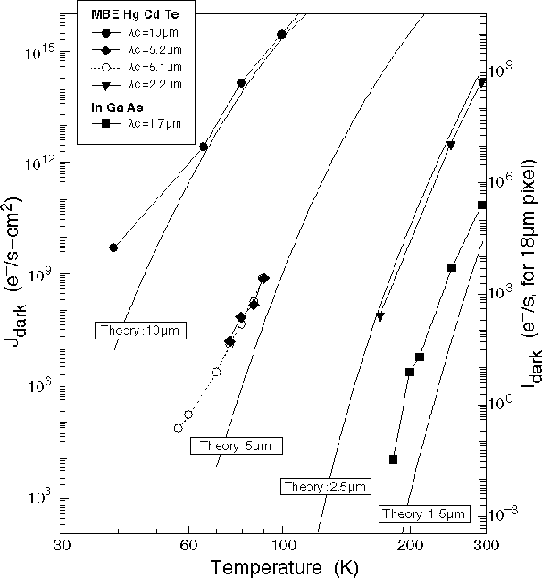
Rockwell has recently achieved a breakthrough in HgCdTe material quality through use of new detector growth technologies which involve p/n double layer planar heterostructure arrays grown by MBE on lattice matched CdZnTe substrates. Initial tests of 256 x 256 arrays of this material have demonstrated near theoretical dark current as a function of temperature and cutoff wavelength (Figure 2). The new material is lattice matched to the CdZnTe substrate, eliminating the lattice defects of earlier PACE material which are thought to be responsible for both its reduced quantum efficiency at short wavelengths and also image persistence effects. In contrast to the low index sapphire substrate used in PACE material, the refractive index of CdZnTe is well matched to the HgCdTe detector material; the exposed surface of the CdZnTe substrate can thus readily be anti reflection coated and Rockwell is now routinely achieving quantum efficiencies in excess of 80% with this technology.
In November 1997, IfA entered into a contract with Rockwell for the development of a 2048 x 2048 format, 18 ![]() m pitch, low noise HAWAII-2 multiplexer (mux) based on the proven HAWAII technology; the European Southern Observatory and the Subaru Telescope have also joined this effort. The first run of this 4 Mpxl mux will take place late summer in the same Rockwell production foundry where high yields of the HAWAII muxes have been consistently achieved. This contract specifies early 1999 delivery of two science grade arrays to UH; they will consist of the 4 Mpxl muxes hybridized to traditional 2.5
m pitch, low noise HAWAII-2 multiplexer (mux) based on the proven HAWAII technology; the European Southern Observatory and the Subaru Telescope have also joined this effort. The first run of this 4 Mpxl mux will take place late summer in the same Rockwell production foundry where high yields of the HAWAII muxes have been consistently achieved. This contract specifies early 1999 delivery of two science grade arrays to UH; they will consist of the 4 Mpxl muxes hybridized to traditional 2.5 ![]() m PACE HgCdTe. Rockwell intends to subsequently offer arrays utilizing this mux to the broad astronomical community. The 37 mm physical dimensions of the 4 Mpxl HgCdTe arrays are only fractionally (one third) larger than the corresponding 27mm of the 1024 x 1024 ALADDIN InSb arrays and the 18
m PACE HgCdTe. Rockwell intends to subsequently offer arrays utilizing this mux to the broad astronomical community. The 37 mm physical dimensions of the 4 Mpxl HgCdTe arrays are only fractionally (one third) larger than the corresponding 27mm of the 1024 x 1024 ALADDIN InSb arrays and the 18 ![]() m pixel size reduces the rate of ionizing events per pixel by better than a factor of two.
m pixel size reduces the rate of ionizing events per pixel by better than a factor of two.
The same muxes can also be readily hybridized to both to Si diode arrays and to MBE HgCdTe material with cutoff wavelengths as long as17 ![]() m, thus providing the option of wavelength coverage from the ultraviolet through much of the MIR. For many applications this offers the flexibility of extended wavelength coverage with the operational simplicity of using the same multiplexers at the same operating temperature..
m, thus providing the option of wavelength coverage from the ultraviolet through much of the MIR. For many applications this offers the flexibility of extended wavelength coverage with the operational simplicity of using the same multiplexers at the same operating temperature..
The planed NGST investigation would consist of the following tasks:
Although the 2048 x 2048 device will be, by a factor of four, the largest device yet fabricated in deep submicron CMOS technology, Rockwell extrapolates high yields based on previous experience with their world-class foundry. The yield of the HAWAII muxes has increased 400% over the last two years and, on the basis of ongoing improvements driven by worldwide competition, we anticipate a defect free yield approaching 30% for the larger muxes.
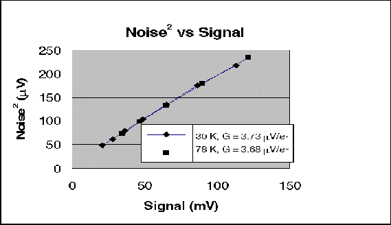
Operation at the 30K temperature of the NGST focal plane represents a significant extrapolation of the 60 - 77K temperatures at which HAWAII muxes have been operated. The lower operating temperature was not anticipated to be a problem and we have confirmed that two critical parameters, gain and read noise, for an engineering grade HAWAII array show no significant change between 78 and 30 K. The results, shown in Figure 1, demonstrate a change of less than 1.5% in mux gain and no measurable change in read noise (23 vs. 22.7 electrons). The performance of both muxes and hybrid arrays at temperatures down to 30k will be fully evaluated during the proposed investigation as described in Section 5..
 |
Rockwell's MBE technology has been shown to produce the best HgCdTe FPA's in the industry spanning cutoff wavelengths from 1.85 to 17.3 ![]() m.
m.
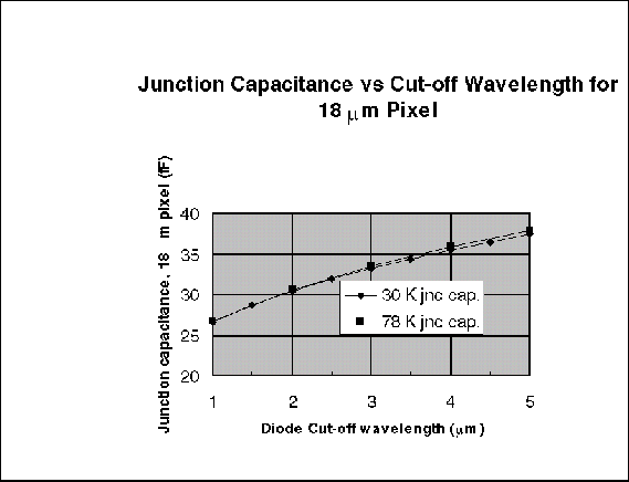
Tailoring ![]() c to shorter wavelengths also improves read noise as the junction capacitance decreases with
c to shorter wavelengths also improves read noise as the junction capacitance decreases with ![]() c. Figure 3 shows the modeled junction capacitance plus input capacitance vs.
c. Figure 3 shows the modeled junction capacitance plus input capacitance vs. ![]() c for an HgCdTe/CdZnTe MBE double layer planar heterostructure (DLPH) diode. The figure shows that the junction + input capacitance is reduced from 37 to 32 fF as
c for an HgCdTe/CdZnTe MBE double layer planar heterostructure (DLPH) diode. The figure shows that the junction + input capacitance is reduced from 37 to 32 fF as ![]() c is reduced from 5 to 2.5
c is reduced from 5 to 2.5 ![]() m and that there is no change in read noise from 78 to 30K.
m and that there is no change in read noise from 78 to 30K.
The main challenge in scaling up the hybrid mating method is the need to apply four times the force to the hybrid components to produce a robust indium interconnect bond. Rockwell's current mating machine is capable of mounting and aligning the larger die of the 2048 x 2048 device, but is not designed to apply the required loads. Our plan for hybridization of the HAWAII-2 arrays is to use this mating machine to align and attach the hybrid components at the load currently used for the 1024 x 1024 arrays, then transfer the hybrid to a very rigid air gimbal in a load frame. Such a compressive apparatus can be made much more rigid than a mating machine, since there is no need to accurately control the movement and orientation of the mounting surfaces. The hybrids will then be compressed to the final load, with the air gimbal ensuring that the load is evenly distributed. The air gimbal and other components for this mating method are in house at Rockwell: the first 2048 x 2048 hybrids are scheduled for fabrication under the HAWAII-2 program late in 1998. Mask sets have also been procured for the fabrication of 2048 x 2048 test structures. The 2048 x 2048 hybrid mating technology should be relatively mature and have been fully demonstrated under the HAWAII-2 program well before 2048 x 2048 arrays would be required for the NGST program.
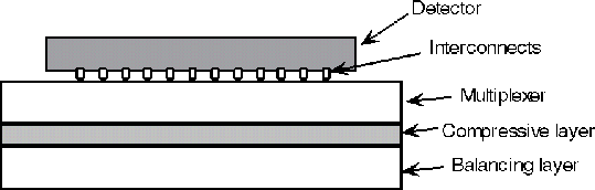
The difference in thermal expansion between the detector and the silicon mux has the potential to create large thermally induced stresses on the indium interconnects and the detector material. With repeated thermal cycling this can result in failure of the interconnects or lead to damage to the detector pixels. Rockwell has developed the Balanced Composite Structure (BCS) design to produce reliable hybrids and applied it to a variety of FPA designs, including the 1024 x 1024 HAWAII FPA. This design relieves the stress at the hybrid interface by compressing the mux to match the thermal expansion of the detector material. The thickness and composition of the compressive layer is adjusted to produce the desired compression of the multiplexer. A balancing layer below the compressing layer prevents bending of the FPA (Figure 4) The BCS design has been successfully applied to a number of FPA's with CdZnTe-substrate detectors and Rockwell does not anticipate the need for any modifications in going to the 2048 x 2048 format hybrids.
 |
We plan to carry out initial characterization of HAWAII-2 engineering grade muxes hybridized to 256 x 256 sub arrays of 5.0, 2.5 and 1.8 ![]() m MBE HgCdTe material on lattice matched CdZnTe substrates and to Si PIN diode arrays. Later we intend to demonstrate and characterize full scale 2048 x 2048 array technology. By that time there will exist a substantial body of data on HAWAII-2 muxes hybridized to traditional PACE material.
m MBE HgCdTe material on lattice matched CdZnTe substrates and to Si PIN diode arrays. Later we intend to demonstrate and characterize full scale 2048 x 2048 array technology. By that time there will exist a substantial body of data on HAWAII-2 muxes hybridized to traditional PACE material.
Typical HgCdTe FPA's are not sensitive to visible wavelengths due to absorption in the CdZnTe substrate layer short of 0.8 ![]() m. It is possible to achieve detector response comparable to InSb in the visible by removing the CdZnTe substrate with a selective etch. At least two standard etches are available that remove the CdZnTe substrate but do not affect the layer containing Hg. This process would remove the entire CdZnTe substrate leaving only the very thin active layer of HgCdTe hybridized to the multiplexer. This material would be sensitive to visible wavelengths.
m. It is possible to achieve detector response comparable to InSb in the visible by removing the CdZnTe substrate with a selective etch. At least two standard etches are available that remove the CdZnTe substrate but do not affect the layer containing Hg. This process would remove the entire CdZnTe substrate leaving only the very thin active layer of HgCdTe hybridized to the multiplexer. This material would be sensitive to visible wavelengths.
Several issues would need to be addressed in this approach:
Rockwell has established technologies which would address all of these issues.
However, the alternate of hybridizing a back-illuminated Si PIN diode array to the 2048 x 2048 mux appears far more attractive. By utilizing this hybrid focal plane array approach, it is possible to produce a visible imager which will operate at 30K with a combination of performance and other features not attainable with either HgCdTe or InSb in the visible. In this hybrid approach, the detector will be independently optimized for visible quantum efficiency, speed and dark current outside of the standard CMOS process, but will use standard high-volume silicon processing techniques. Due to the maturity of silicon and the available material quality, the cosmetic quality of this device should be very high. The fully-depleted architecture provides low cross-talk and reduces any resistivity variations to improve uniformity of response. This hybrid approach allows for a fill factor of nearly 100%; with an anti-reflection coating of SiO2 tailored to the appropriate thickness, quantum efficiencies exceeding 80% throughout the visible should be achievable. If lower dark current than the thinned wafer approach is required, a bonded-wafer approach in which a thin (10 - 75 ![]() m) silicon layer is transferred to the multiplexer through bump-bonding with the later removal of the thicker bonded substrate can be employed. In this approach dark currents at the levels of CCD's are attainable, while providing the advantages of operation at 30K, utilization of the same 2048 x 2048 multiplexer and non destructive readout.
m) silicon layer is transferred to the multiplexer through bump-bonding with the later removal of the thicker bonded substrate can be employed. In this approach dark currents at the levels of CCD's are attainable, while providing the advantages of operation at 30K, utilization of the same 2048 x 2048 multiplexer and non destructive readout.
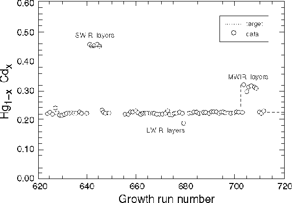
The ability to fabricate MBE HgCdTe with a variety of ![]() c's matched to the science requirements is a key advantage of HgCdTE over fixed band-gap materials. An important attribute of Rockwell's process is the ability to precisely control the band-gap for any run and to rapidly modify it from one run to another. This is illustrated in Figure 7 which documents the growth of a series of LWIR, MWIR and SWIR layers which were grown sequentially demanding the high composition control flexibility inherent to this technology.
c's matched to the science requirements is a key advantage of HgCdTE over fixed band-gap materials. An important attribute of Rockwell's process is the ability to precisely control the band-gap for any run and to rapidly modify it from one run to another. This is illustrated in Figure 7 which documents the growth of a series of LWIR, MWIR and SWIR layers which were grown sequentially demanding the high composition control flexibility inherent to this technology.
Rockwell is currently using MBE processes to produce many arrays. These include all LWIR FPA's (![]() c up to 17.3
c up to 17.3 ![]() m), key MWIR deliverables for operation at elevated temperatures and all NIR (1.8 to 2.3
m), key MWIR deliverables for operation at elevated temperatures and all NIR (1.8 to 2.3 ![]() m) prototypes. The performance benefits of the DLPH MBE HgCdTe detector technology are illustrated by the dark current density data shown in Figure 2 for recent devices with
m) prototypes. The performance benefits of the DLPH MBE HgCdTe detector technology are illustrated by the dark current density data shown in Figure 2 for recent devices with ![]() c from 2.2 to 16
c from 2.2 to 16 ![]() m. The MBE dark current is far superior to traditional PACE material and is in good agreement with the theoretical limit for conventional (unthinned) p/n HgCdTe detectors.
m. The MBE dark current is far superior to traditional PACE material and is in good agreement with the theoretical limit for conventional (unthinned) p/n HgCdTe detectors.
 |